Email:export@yangxing.hk

RX8900CE
FIXED FREQUENCIES: 32.768KHz
DIMENSIONS: 3.2 x 2.5 mm
PACKAGE: 2000 pieces/Reel
ROHS STATUS: Compliant
PN: X1B000301000200 X1B000301000212
DIMENSIONS: 3.2 x 2.5 mm
PACKAGE: 2000 pieces/Reel
ROHS STATUS: Compliant
PN: X1B000301000200 X1B000301000212
Block diagram

Overview
- High Stability
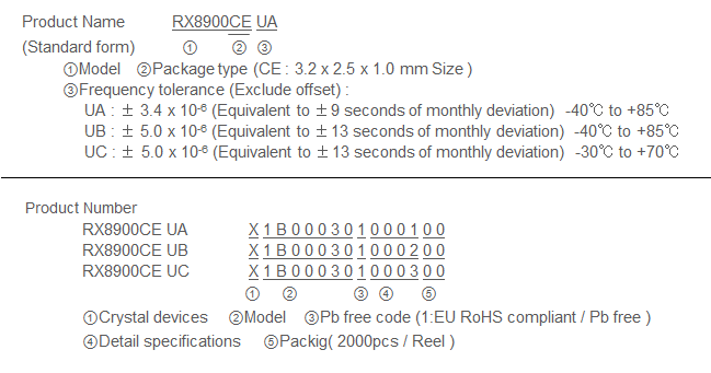
- UA ± 3.4 x 10⁻⁶ / -40 °C to +85 °C ( Equivalent to ±9 seconds of month deviation )
- UB ± 5.0 x 10⁻⁶ / -40 °C to +85 °C ( Equivalent to ±13 seconds of month deviation )
- UC ± 5.0 x 10⁻⁶ / -30 °C to +70 °C ( Equivalent to ±13 seconds of month deviation )
- 32.768 kHz frequency output function
- FOUT pin output (C-MOS output), CL=30 pF
- Output selectable: 32.768 kHz, 1024 Hz, 1 Hz
- Available automatic battery backup switch-over function
- Charge from VDD to backup battery connected to VBAT is possible.
VDD voltage drop(VDET3) detection and automatically switches to the backup battery.
This circuit is optimal to backup with a secondary battery and a large capacitor.
- Charge from VDD to backup battery connected to VBAT is possible.
- Timer function
- Timer period is adjustable in 1/4096 second from 4095 minutes
- Alarm function
- Available dual-alarm, weekly and monthly
- Temp. sensor function
- Available readout temperature data from embedded temp sensor. (Bank.2_Add17h)
Specifications (characteristics)
Refer to application manual for details.
Electrical Characteristics
| Item | Symbol | Conditions | Min. | Typ. | Max. | Unit | ||
|---|---|---|---|---|---|---|---|---|
| Operating voltage | VDD | Interface voltage | 2.5 | 3.0 | 5.5 | V | ||
| Temp. compensated Voltage | VTEM | Temp. compensated voltage | 2.0 | 3.0 | 5.5 | V | ||
| Clock supply voltage | VCLK | Internal clock | 1.6 | 3.0 | 5.5 | V | ||
| Operating temperature | TOPR | No condensation | -40 | +25 | +85 *3 | °C | ||
| Stability | Δ f/f | UA | Ta=-40°C to+85°C | ±3.4 *1 | x10-6 | |||
| UB | Ta=-40°C to+85°C | ±5.0 *2 | ||||||
| UC | Ta=-30°C to+70°C | |||||||
| Current consumption(1) | lDD1 | fSCL=0Hz,/INT=VDD, FOE=GND, VDD=VBAT FOUT:OFF Temp. Compensation interval 2.0 s. |
VDD=5V | - | 0.72 | 1.5 | µA | |
| Current consumption(2) | lDD2 | VDD=3V | - | 0.70 | 1.4 | |||
*1 Equivalent to ±9 seconds of month deviation.
*2 Equivalent to ±13 seconds of month deviation.
*3 Please contact us about +85°C < TOPR
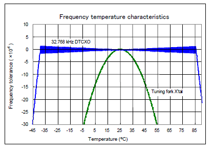
32.768 kHz-DTCXO Frequency temperature characteristics (Example)


Pin function
| Signal Name | I / O | Function |
|---|---|---|
| T1(CE) | input | Use by the manufacture for testing. ( Do not connect externally.) |
| SCL | input | Serial clock input pin. |
| FOUT | output | The pin outputs the reference clock signal. ( CMOS output ) |
| VBAT | - | Battery supply. This pin has charge capability to backup battery. |
| VDD | - | Connected to a positive power supply |
| FOE | input | The input pin for the FOUT output control. |
| / INT | output | Interrupt output (N-ch. open drain). |
| GND | - | Connected to a ground |
| T2(VPP) | - | Use by the manufacture for testing. ( Do not connect externally.) |
| SDA | I/O | Data input and output pin. |
Terminal connection/External dimensions

(Unit: mm)
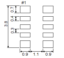
Footprint (Recommended)

(Unit: mm)
To maintain stable operation, provide a 0.1uF by-pass capacitor
at a location as near as possible to the power source terminal of the crystal product (between Vcc - GND).
 Download PDF


