Email:export@yangxing.hk

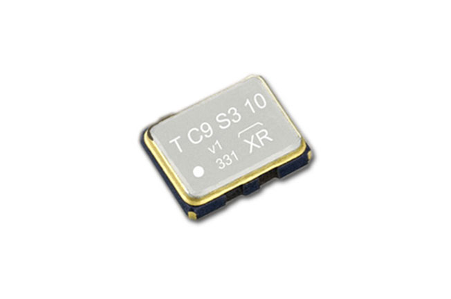
TG-5006CE
Temperature Compensated Crystal Oscillator
Type: Active Crystal Oscillator
Frequency Range: 13MHz-40MHz
External Dimensions: 3.2*2.5mm (3225)
PN: X1G004201001000 X1G004201002500
Application: Wireless communication devices(CDMA, WCDMA, LTE, WIMAX)
Type: Active Crystal Oscillator
Frequency Range: 13MHz-40MHz
External Dimensions: 3.2*2.5mm (3225)
PN: X1G004201001000 X1G004201002500
Application: Wireless communication devices(CDMA, WCDMA, LTE, WIMAX)
| Item | Symbol | Specifications | Conditions/Remarks | |
|---|---|---|---|---|
| VC-TCXO | TCXO | |||
| Output frequency range | f0 | 13.000 MHz to 20.000MHz 26.000 MHz to 40MHz |
||
| 16.367667 MHz, 16.368 MHz, 16.369 MHz 19.2 MHz, 26 MHz and 38.4 MHz |
Standard frequency | |||
| Supply voltage | VCC | 1.8 V ±0.1 V / 2.8 V ± 5 % / 3.0 V ± 5 % / 3.3 V ± 5 % | (Supply voltage range: 1.7V to 3.465V) | |
| Storage temperature | T_stg | -40°C to +90°C | Store as single product. | |
| Operating temperature | T_use | -30°C to +85°C | ||
| Frequency tolerance | f_tol | ±2.0 x 10⁻⁶ Max. | After reflow, VC=0.9V, +25°C | |
| Frequency/temperature characteristics | fo-TC | ±0.5 x 10⁻⁶ Max./-30 °C to +85 °C | High stability version for GPS | |
| ±2.0 × 10⁻⁶ Max./-30 °C to +85 °C | Standard stability version | |||
| Frequency/load coefficient | fo-Load | ±0.2 × 10⁻⁶ Max. | 10kΩ // 10pF ±10% | |
| Frequency/voltage coefficient | fo-VCC | ±0.2 × 10⁻⁶ Max. | VCC ± 5 % | |
| Frequency aging | f_age | ±1.0 × 10⁻⁶ Max. | +25°C, First year | |
| Current consumption | ICC | 1.5mA Max. | 13 MHz≤f0≤26 MHz | |
| 2.0mA Max. | 26 MHz | |||
| Input resistance | Rin | 500kΩ Min. | - | VC- GND (DC) |
| Frequency control range | f_cont | ±5.0 × 10⁻⁶ to ±12.0 ×10⁻⁶ | - | VC=0.9V ± 0.6V (Vcc =1.8 V) or VC=1.4 V ±1.0 V (Vcc =2.8 V) |
| Frequency change polarity | - | Positive polarity | - | |
| Symmetry | SYM | 40% to 60% | GND level (DC cut) | |
| Output voltage | VPP | 0.8V Min. | Peak to peak | |
| Output load condition | Load_R | 10kΩ | DC cut capacitor = 0.01µF | |
| Load_C | 10pF | |||
* Note : Please contact us for inquiries about specifications other than the above.

External dimensions

(Unit: mm)
Please keep "N.C." pin OPEN condition or GND connection.
"N.C." pin doesn’t work as a ground pin.
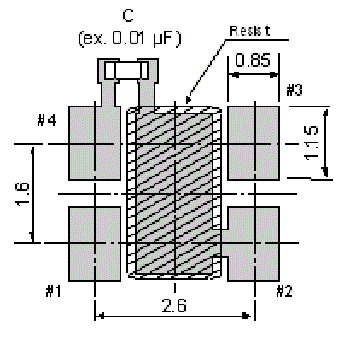
Footprint (Recommended)

(Unit: mm)
For stable operation, please add a bypasscapacitor (0.01uF to 0.1uF) between Vcc and GND.
Please place it as close to TCXO as possible.
 Download PDF


